How AI is Creating the Cognitive Luminaire
28 Apr, 2026

What raw materials are needed for semiconductors?Semiconductors are made from a variety of r...
Semiconductors are made from a variety of raw materials, including silicon, germanium, gallium arsenide, and indium phosphide. These materials are processed and purified to create a crystalline structure, which forms the foundation for building semiconductor devices such as transistors, diodes, and integrated circuits.
Other raw materials used in the manufacture of semiconductors include impurities such as boron and phosphorus for doping, as well as metals for interconnects, insulators for isolation, and various chemicals for cleaning and etching.
Semiconductors are manufactured through a complex process that involves multiple steps, starting from the preparation of raw materials and ending with the production of finished devices.
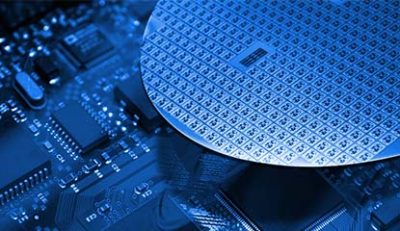
The process begins with the preparation of raw materials. As mentioned above, there are several raw materials that are used in the manufacturing process. However, the fundamental buildng block is silicon. This accessible and processable material is melted to create silicon boule's. The boule's are then cut into thin wafers, typically around 0.75mm thick.
For these wafers to be manufactured into p-type and n-type semiconductors, impurities such as boron or phosphorus are added. This process is known as doping. P-type semiconductors have an excess of holes, while n-type semiconductors have an excess of electrons. When the p-type and n-type semiconductors are brought together, they form a p-n junction, which is the foundation for many semiconductor devices.
After the doping process, a thin layer of silicon dioxide is layered on the surface of the wafer by exposing it to oxygen in a high-temperature furnace. This layer acts as an insulator, protecting the surface from electrical charges and providing a stable base for further processing.
Next, a mask is created and used to define the pattern for the active devices. A light-sensitive material, called photoresist, is applied to the wafer. The wafer is then exposed to light through the mask, which hardens the photoresist. The unexposed photoresist is then removed, leaving a pattern on the wafer.
The pattern is then transferred to the surface of the wafer by etching, which removes the unprotected silicon dioxide and semiconductor material. The etching process is carefully controlled to ensure that the desired shapes and dimensions are produced.
Thin films of metal and insulators are deposited on the wafer to create interconnects and insulators. The metal films are used to create electrical connections between the active devices, while the insulator films provide electrical isolation and protect the devices from external damage.
The individual devices are then separated and assembled into packages. The packages may be as simple as a metal lead frame or as complex as a multichip module. Thereafter, the completed devices are thoroughly tested to ensure they meet the required specifications. This may include testing for performance, reliability, and electrical characteristics.
From here, the tested devices are packaged in a protective material, such as a plastic or ceramic package, and prepared for shipment.
On average, the fabrication process can take anywhere from a few weeks to several months, depending on the specific requirements of the semiconductor device being produced. It's important to note that the semiconductor fabrication process is a complex and highly technical process that requires specialized equipment, facilities, and trained personnel.
Due to this, the fabrication of a semiconductor can take anywhere from several weeks to three months. Therefore, it’s important for companies that manufacture semiconductors to take this into consideration, as it can impact production schedules and costs.
Technological advancements have resulted in improvements in the semiconductor manufacturing process and materials used, which has contributed to increased reliability and performance in semiconductors, as well as their overall lifespan.
Semiconductors are made from materials such as silicon, germanium, and gallium arsenide, which have improved in quality and purity, leading to better performance and longer lifetimes. In addition, advancements in fabrication technologies, such as photolithography and deposition techniques, have enabled the production of smaller, more complex, and higher-performance devices.
Moreover, improved design techniques and better quality control during the manufacturing process have also contributed to a longer lifespan of semiconductors. Newer materials, such as wide bandgap semiconductors, have also been developed that are able to withstand higher temperatures and operate at higher voltages, which can result in longer lifetimes.
It's worth noting that while the lifespan of semiconductors has improved, they are still susceptible to degradation and failure over time. The lifespan of a semiconductor can vary widely, with some breaking down after two years, while others last for as long as twenty. However, technological advancements continue to push the limits of performance and reliability, leading to even longer lifetimes for semiconductors in the future.
If you enjoyed this article and want to talk about your career in semiconductor manufacturing, you may want to get in touch. At MRL, we’ve been recruiting for the semiconductor industry for over 25 years. Our extensive experience has made us a market leading recruitment consultancy. If you’d like to learn more about this industry and how we can help you, feel free to get in touch.