How are Semiconductors Made?
29 Apr, 2025
The semiconductor industry is highly competitive, with companies constantly designing ...

The semiconductor industry is highly competitive, with companies constantly designing smaller and more powerful chips. The demand for small and powerful has led to rising costs for research and development and production equipment. AI (artificial intelligence) can help companies optimise their operations by analysing losses at every production phase. For companies working with next-generation, more expensive semiconductor materials, the ability to assess even the slightest of losses is paramount.
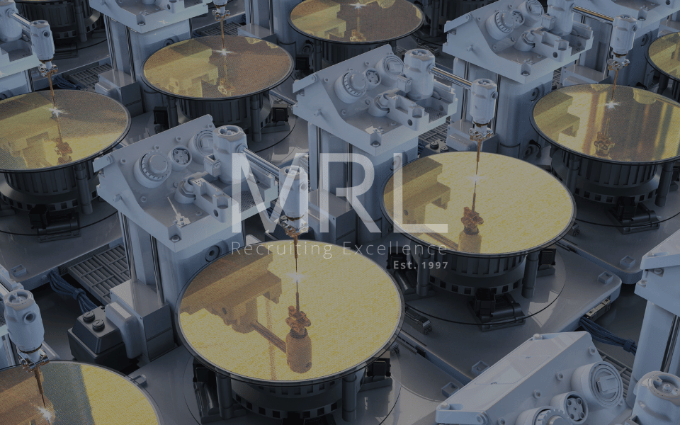
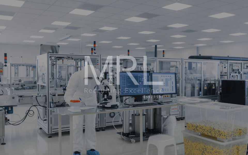
Most typically, AI is found in the manufacturing side of the industry, with large parts of the manufacturing process being automated using AI and machine learning algorithms. From machines that transport the wafers across fabs to those used to identify defects in wafers, AI has become an integral part of the industry.
It's no wonder this is the case as the semiconductor industry stood to gain significant value from the integration of AI into its processes. From design and development to manufacturing and analysis, AI has the potential to improve every step of the production cycle. The COVID-19 pandemic has only accelerated the shift towards digitisation.
McKinsey reports that only 30% of companies are currently seeing value from AI/ML (artificial intelligence/ machine learning) at a current contribution of $5 billion to $8 billion. McKinsey goes on to predict that the application of these technologies could generate USD$85 billion to USD$95 billion in the long term. Companies that invest in scaling AI now will be better positioned to remain competitive.
The inspections of wafers can be improved with AI-powered computer vision systems that accurately identify and classify defects. This not only improves yields but also saves costs by detecting problems earlier. AI has already seen high adoption rates in product and service development and operations, with reported revenue increases in areas such as inventory and parts optimisation, customer service analytics, and sales and demand forecasting.
In light of the COVID-19 pandemic, which created an imbalance in the supply chain, semiconductor companies are seeking to diversify their supplier base and minimise risks through the use of AI. Digital and machine learning solutions can improve visibility into suppliers, optimise capacity, and proactively manage supply chain risks. By leveraging AI algorithms in procurement and material planning, companies can gain insights into supply and demand and improve their planning cycle, leading to enhanced supply chain resilience and cost savings.
In the sales and marketing domain, the growing demand for smart devices has driven the need for semiconductor manufacturers to understand consumer buying patterns. AI can analyse data to streamline the demand-supply gap and guide effective sales and marketing through lead management, pricing, and promotions. Anticipating supply problems and predicting unexpected events is another area where AI can provide valuable insights to the semiconductor industry.
Whilst we've only scratched the surface, it is clear to see that AI in the semiconductor industry has many applications that present various opportunities to drive value and increase competitiveness. Whilst it is a high-cost investment, it's also a highly beneficial one that could provide significant returns in the first five years of adoption. It is imperative for companies in this industry to implement an AI strategy to stay ahead of competition.
We have clients across the USA and Europe building state of the art fabs, and they all need staffing. If you're interested in talking about an opportunity in a state of the art manufacturing facility, then get in touch with our head of manufacturing, lauren.hart@mrlcg.com and she'll talk to you about all of the opportunities we're currently hiring for.