How are Semiconductors Made?
29 Apr, 20255 minsAt the forefront of modern technology is the semiconductor industry. Everything from compute...

At the forefront of modern technology is the semiconductor industry. Everything from computers and smartphones to automobiles and medical equipment is powered by it. However, not many people are sure of the production and manufacturing processes involved. The process combines engineering, physics, and chemistry and calls for extreme precision. We’re here to break down the steps on just exactly how these small but powerful chips are created!
Step 1: Raw Silicon Extraction
The first step in making semiconductors is finding the right material. They mainly use silicon, which comes from sand. But not all silicon works for making semiconductors. It begins with extracting silicon from quartzite, a type of high-quality sand. This silicon is then refined through a process known as the Czochralski method. It is slowly melted and pulled into a single cylindrical crystal called an ingot.
Step 2: Wafer Fabrication
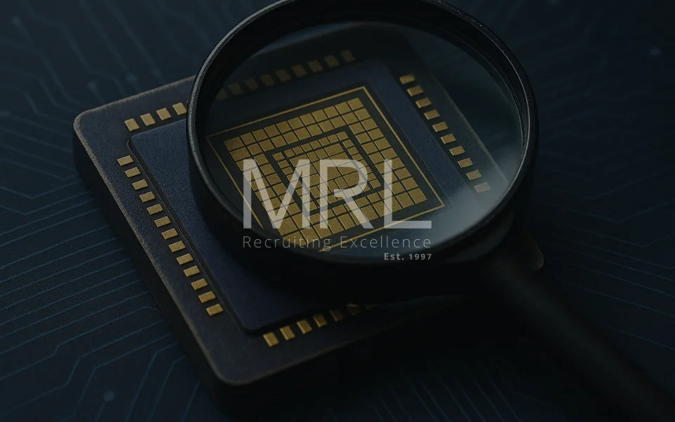
When the silicon ingot has been formed, it is then sliced into disc-shaped wafers using diamond-tipped saws. These wafers are extremely thin, often just a fraction of a mm thick. The wafers undergo a series of polishing and cleaning to remove imperfections and contaminants. The result is a perfect, mirror like surface to house the semiconductor circuits.
Step 3: Doping
To create working semiconductor devices, manufacturers now undergo a process known as doping. This is where controlled impurities are added to the silicon. This step alters the electrical properties of the silicon, which makes it possible to control how electricity flows through the material. Depending on the requirement, elements such as phosphorus or boron are used to create p-type or n-type semiconductors.
Step 4: Photolithography
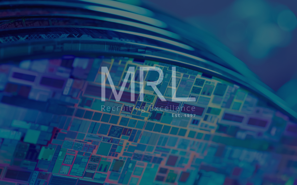
Once the silicon wafer has been prepared as above, the intricate design of a semiconductor chip is created using photolithography. A light-sensitive chemical called photoresist is added to the wafer's surface. Ultraviolet light is projected through a mask, which prints the circuit pattern onto the wafer. As there are complex layers of circuits that make up a semiconductor chip, this process has to be repeated multiple times.
Step 5: Etching and Deposition
Etching – by either chemical (wet etching) or plasma (dry etching), removes the unwanted material after the circuit pattern is printed. Meanwhile, additional layers of insulating and conductive material are added onto the wafer to create transistors and interconnections. These layers are most important in determining the performance of the semiconductor.
Step 6: Testing and Packaging
Now that the wafers are fully processed, they are sliced into individual semiconductor chips. Each chip undergoes testing to ensure it functions correctly. Any chip that is faulty gets thrown away. Working chips are wrapped in protective packaging and fitted with electrical contacts. This gets the chips ready for integration into electronic devices.
The semiconductor manufacturing process is leading the way in modern engineering. The semiconductor industry continues to push the boundaries of innovation, which leads to faster, smaller, and more efficient chips that help to power the digital world. As demand for advanced technology grows, so does the need for more sophisticated and powerful semiconductor fabrication techniques. With ongoing research and development, the future of semiconductors promises even bigger breakthroughs in computing, artificial intelligence, and beyond!
Get in touch with MRL to begin your move into your future semiconductor career.